 |
| February 25, 2014 | Volume 10 Issue 08 |
Designfax weekly eMagazine

Archives
Partners
Manufacturing Center
Product Spotlight
Modern Applications News
Metalworking Ideas For
Today's Job Shops
Tooling and Production
Strategies for large
metalworking plants
What NASA is doing with 3D printing:
Goddard reaching new potential with additive manufacturing
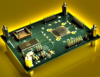
This is a close-up of the housekeeping chip that was bonded onto an electronics board as part of an investigation into the effectiveness of 3D manufacturing for electronics applications. Image Credit: [NASA]
By Lori Keesey, NASA's Goddard Space Flight Center, Greenbelt, MD
For the past two years, the Internal Research and Development, or IRAD, program at NASA's Goddard Space Flight Center in Greenbelt, MD, has awarded funding to a small number of researchers who are investigating how the agency might benefit from additive manufacturing.
Additive manufacturing, or "3D printing," is an emerging technology where computer-operated devices literally print solid objects from powdered metals or some other material, layer by layer until they are complete.
"We're not looking to reinvent the wheel or pursue applications that industry already can do with 3D manufacturing," says NASA Goddard Chief Technologist Peter Hughes. "We're interested in finding out how this technology can enhance NASA's ability to create one-of-a-kind instruments and components geared exclusively to studying and operating in space; in other words, improve what we already do well."
Thermal control
One area that could potentially benefit from 3D manufacturing is electronics, particularly the techniques that technologists use to remove heat from heat-sensitive computer chips.
"There is room for optimism," says Principal Investigator Jeffrey Didion, a researcher at NASA Goddard who is involved in a comprehensive, multi-year effort to advance electrohydrodynamic (EHD)-based thermal control for removing heat from spacecraft electronics.
Unlike traditional thermal-control technologies that rely on mechanical pumps and other moving parts, EHD uses electric fields to pump coolant through tiny ducts inside a thermal cold plate. From there, the waste heat is dumped onto a radiator and dispersed far from heat-sensitive circuitry that must operate within certain temperature ranges. The advantages are many. Without mechanical parts, the system is lighter and consumes less power and space.
Perhaps more importantly, the system can be scaled to different sizes because mechanical hardware no longer drives the size or placement of the system within an electronics box.
A version of Didion's thermal-control device is being demonstrated right now on the International Space Station. In addition, Didion carried out two validation experiments last year, one under variable gravity and the other during a sounding-rocket mission. During these experiments, he also demonstrated the usefulness of a battery case made of Polyetherketoneketone, or PKK, the first 3D-printed part Goddard has flown.
Didion is continuing to investigate how he might use additive manufacturing to integrate EHD into the electronics board itself.
"What we'd like to do is look at integrating thermal management into a functioning electronics board," Didion says. "In theory, we could do a better job of packaging devices and reducing mass, power consumption, and volume" -- a notable endeavor given NASA's push to reduce instrument size and fly a greater number of less-expensive CubeSats and other smaller spacecraft.
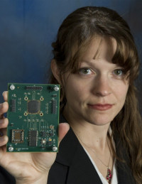
Beth Paquette received IRAD funding to advance a common customizable instrument electronics package called MinE Pack. [Image Credit: NASA]
Electronics packaging
To that end, Didion has joined forces with NASA Goddard Principal Investigator Beth Paquette, who received IRAD funding to advance a common customizable instrument electronics package called MinE Pack. The device would combine different functions inherent in all instruments -- housekeeping, data processing, power, digitization, control and data handling, and amplification -- all onto a single three-dimensional chip or stack of chips.
"Our goal is to have all functions packaged into a component that could be plugged into a board or instrument," Paquette says. "To help us get there, we plan to use additive manufacturing that could print conductors from chip to substrate."
Last year, Paquette focused on advancing MinE Pack's possible "housekeeping" function using the NASA Goddard-developed "Housekeeping-System-on-a-Chip," a structured, radiation-hardened application-specific integrated circuit designed to monitor everything from voltages and currents to temperature levels, all while consuming less than half a watt of power. Working with the chip's creator, George Suarez, she defined the process for bonding the housekeeping chip onto a printed wiring electronics board.
"The future is looking to additive manufacturing techniques in electronics packaging. This opens up a lot of opportunities for miniaturized packaging, while decreasing the costs of spacecraft electronics," she says.
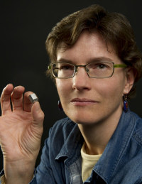
Jean-Marie Lauenstein is holding a printed Inconel-625 spot shield she created for an electronic component. Lauenstein is using 3D manufacturing to protect sensitive circuitry from space radiation. [Image Credit: NASA]
Electronics shielding
NASA Goddard Principal Investigator Jean-Marie Lauenstein also is investigating the use of 3D printing to solve another electronics challenge: protecting sensitive circuitry from damage caused by exposure to space radiation.
"Dosages from radiation can degrade performance to the point where the electronics no longer work," she explains. To protect them, instrument developers currently house sensitive components inside an electronics box made of metal. The thickness of that box depends in part on how much radiation the components are expected to encounter. Although the technique is effective, it "adds a tremendous amount of mass," she says. Engineers also use "spot shielding," which usually involves placing a slab of metal over the part.
Lauenstein says she believes 3D printing offers an intriguing alternative because the protective metal could be printed selectively to enclose the part, minimizing volume and maximizing protection.
Lauenstein used a computer code that not only calculated how much shielding a component required on a given side, but also created a CAD drawing that a 3D printer then used to build the shielding. "We print shields tailored for specific package types for a hand-and-glove fit to minimize mass and area," she says.
This year, Lauenstein's team plans to continue tests to make sure the printed shields can withstand the harsh environmental conditions encountered during launch and in space.
So far, Lauenstein is optimistic, believing 3D printing -- and more precisely, a technique called direct metal laser sintering -- could allow instrument developers in the future to use more state-of-the-art, non-radiation-hardened circuits and rely less on mass-intensive, box-level shielding. "We hope this will become one more tool in the toolbox for mitigating radiation-dose effects," she says.
Optical benches and telescopes
Direct metal laser sintering also may benefit instrument structures, according to NASA Goddard Principal Investigator and Technologist Tim Stephenson. Working with the Michigan-based EOS of North America, Inc., he developed the world's first Invar structure produced by this technique, which literally prints objects from powdered metals.
Invar is weak and bends easily. However, it is stable and nearly immune to shrinkage or expansion due to extreme changes in temperature. As a result, it is ideal for optical benches and other instrument structures that demand stability. In fact, nearly a half-ton of the material was used to build the James Webb Space Telescope's Integrated Science Instrument Module, upon which the observatory's instruments hang. "Our goal is to see if we can lightweight these kinds of spacecraft structures through direct metal laser sintering," Stephenson says.
He's upping the ante this year.
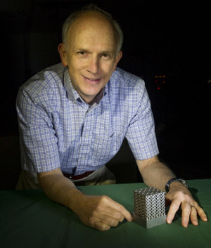
Principal Investigator Tim Stephenson worked with EOS of America, Inc., to develop the first 3D-manufactured object made with Invar, a material especially useful for optical benches due to the material's immunity from shrinkage and expansion caused by temperature changes. [Image Credit: NASA]
Stephenson is working with NASA Goddard astrophysicists to produce engineering prototypes satisfying the stability requirements for a coronagraph capable of detecting planets beyond the solar system. He also is fabricating a prototype cavity for the proposed Laser Interferometer Space Antenna, a concept to detect gravitational waves by monitoring the distance between three spacecraft.
"The versatility inherent in additive manufacturing greatly expands an engineer's pallet," Stephenson says. "Fabrication of a complete CubeSat/MicroSat bus in a single step is now possible."
Jason Budinoff, another NASA Goddard technologist, has teamed with Stephenson to use direct metal laser sintering to fabricate proof-of-concept, fully integrated 3D-printed telescopes. The goal is to not only decrease the costs and time needed to fabricate and align instrument assemblies, save mass, and increase dimensional stability, but also to drastically slash part counts and interfaces -- a challenge that this technique could meet, Budinoff says. Ultimately, he wants to gain experience with the technology and familiarize more engineers with the unique design considerations that 3D manufacturing requires.
His ambitions mirror those of Ted Swanson, assistant chief for technology for Goddard's Mechanical Systems Division. "My mission is to get the word out about this technology. We're only limited by our imaginations as to how we can use this technology to make our instruments and components smaller, cheaper, and better. This is just the start. This technology is developing so fast, it's hard even for us to stay on top of it," says Swanson.
Published February 2014
Rate this article
View our terms of use and privacy policy